Welcome to techinsights.com
Looking for general Manufacturing Analysis (formerly VLSIresearch) content?
April 20th onwards, visits to vlsiresearch.com have been redirected to TechInsights.com.
All product information can be found under Market Analysis: Manufacturing Analysis.
- VLSI Releases is now called Industry Releases
- VLSI Papers is now located under News & Articles
- WeVision and VLSIinsiders is now under Insights
You will require new credentials to access the TechInsights Platform. If you did not receive an email with your activation instructions, or if you require assistance in creating your new credentials, please reach out to support@techinsights.com
Are you a subscriber to Manufacturing Analysis?
All VLSIresearch subscribers are encouraged to access their Manufacturing Analysis subscription from the TechInsights Platform via the Platform login at techinsights.com
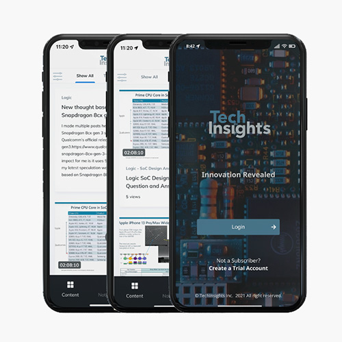
Mobile App update
The VLSI mobile app will also be sunset after April 20, 2022.
You can download the TechInsights mobile app from Google Play or Apple Store to get the latest tech news, analysis, and market intelligence.


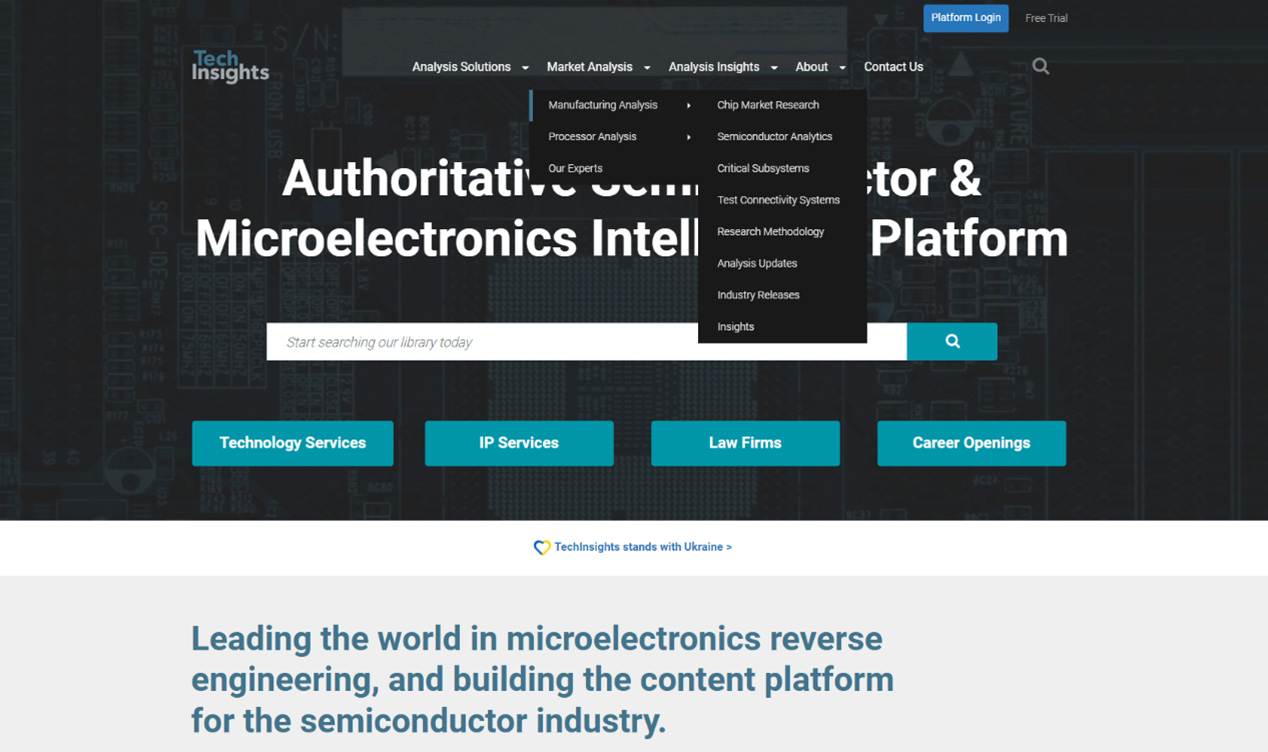
The authoritative information platform to the semiconductor industry.
Discover why TechInsights stands as the semiconductor industry's most trusted source for actionable, in-depth intelligence.
